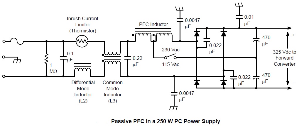
Passive PFC Circuit for 250W PC Power Supply
The circuit show here is input circuitry of the power supply with passive PFC. Note the line voltage range switch connected to the center tap of the PFC inductor. In the 230V position (switch Open) both halves of the inductor winding are used and the rectifier functions as a full wave bridge. in the 115V ( switch closed) position only the left half of the inductor and left half of the rectifier bridge are used, placing the circuit in the half wave double mode. As in the case of the full wave rectifier with 230V AC input, this produces 325V DC at the output of the rectifier. This 325 VDC bus is , of course, unregulated and move up and down with i9nput line voltage.
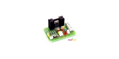
Circuit Courtesy www.onsemi.com
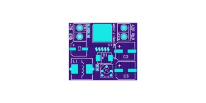
EMI FILTER CIRCUIT FOR 110V AC INPUT
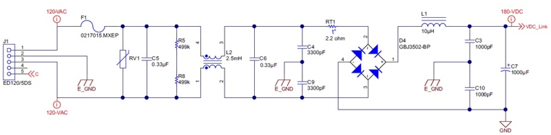
The AC-DC power stage is shown in Figure 6. The connection port is set up identical to the ECM motor controller port for ease of testing. The common is the output port for the control signal 24-V AC inputs. The other input/output ports are for the hot, neutral, and earth ground connections. This TI Design also incorporates a 15-A 250-V AC rated fuse to prevent damage to the board in case of overcurrent. The RV1 metal oxide varistor (MOV), rated for 275-VRMS, is also used for surge protection. Both 499-kO resistors are used as the discharge resistive network for capacitors C5 and C6, and are rated for 400 V. The rectification bridge is rated for 200 V at 35 A, leaving plenty of room for a sufficient safety
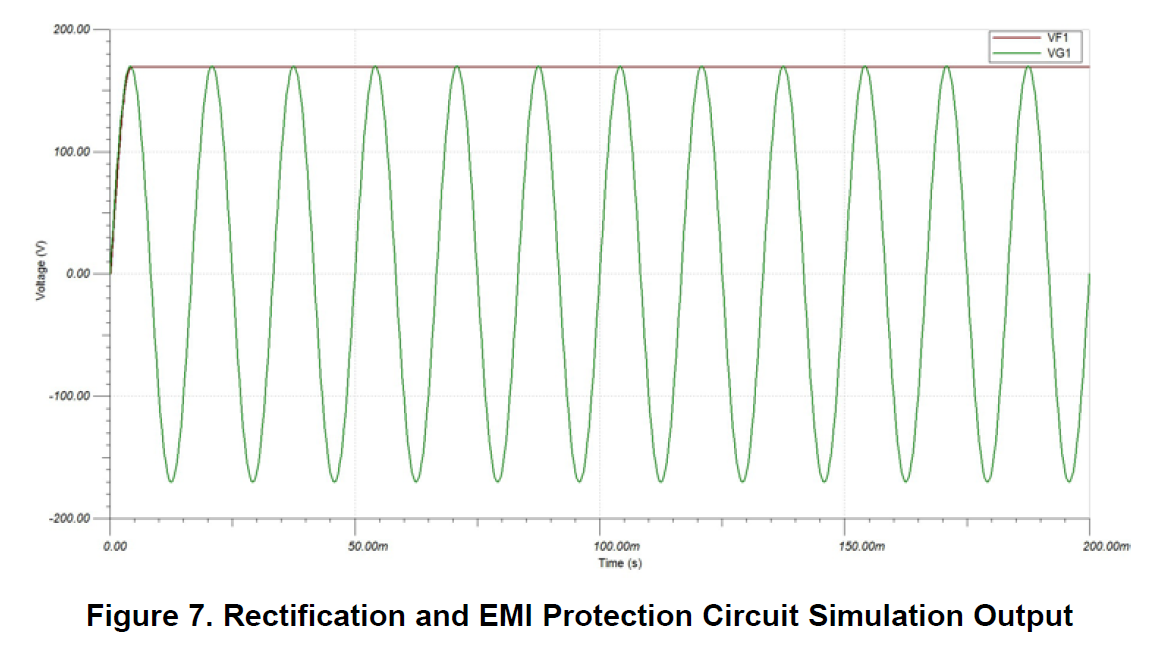
factor. L2 is a common-mode filter. To limit the inrush current of the bulk DC capacitors, an inrush current limiter RT1 is provided. D4 is the full bridge rectifier. L1 is the DC choke provided for meeting the line harmonic standard. C7 is the electrolytic capacitor at the DC bus. The AC-DC subsection of the design has been designed with the DC bus capacitor and necessary filters for conducted emission, surge, and EFT protection as per the standard EN55014. Figure 7 shows the simulation output of the design using the listed circuit parameters.To reduce the voltage ripple of the DC output, calculate the bulk capacitor or DC link capacitor value. This helps ensure that a sufficient hold up time is provided, during which the regulated supply continues to provide the regulated voltage output in the event of a short lapse in AC voltage supply. The following arithmetic is used to properly fit the circuit with an appropriately sized DC bus capacitor.