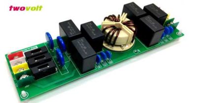
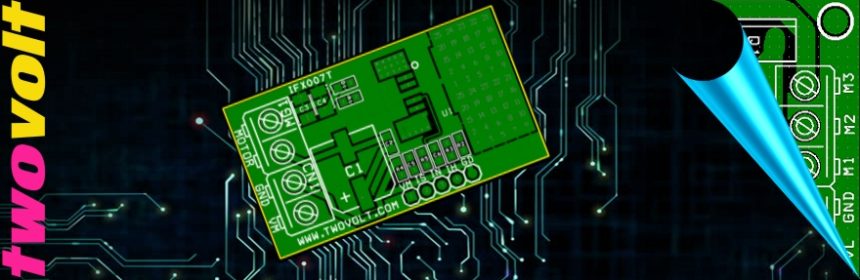
High Current Half Bridge DC Motor Driver with Integrated Driver IFX007
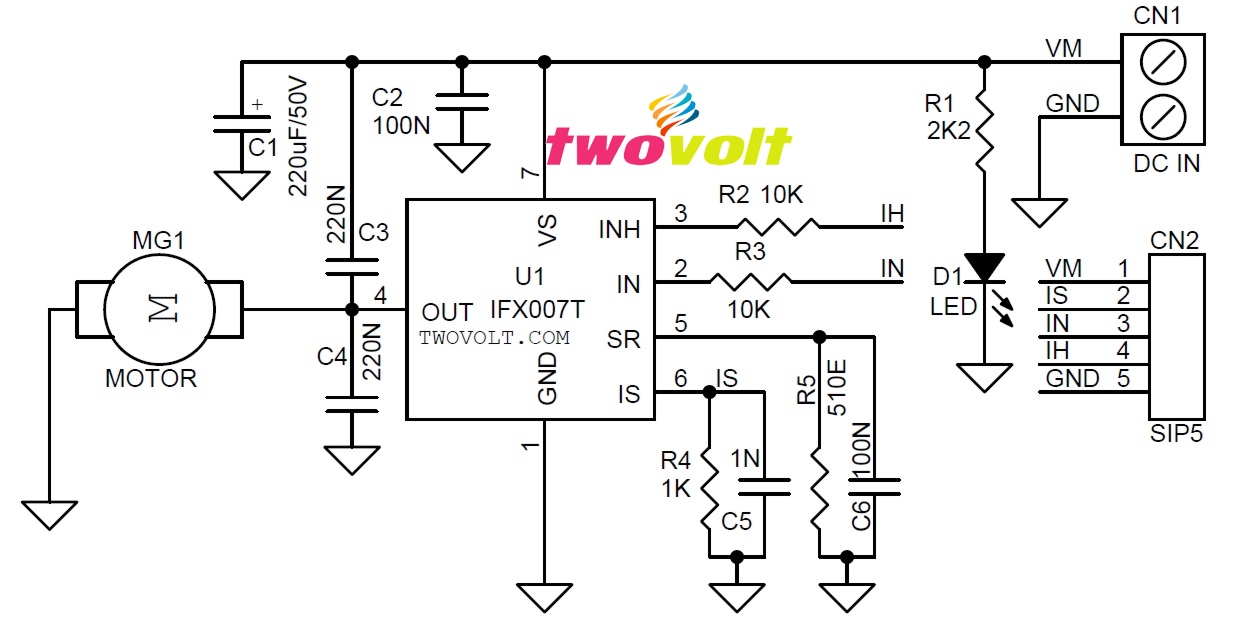
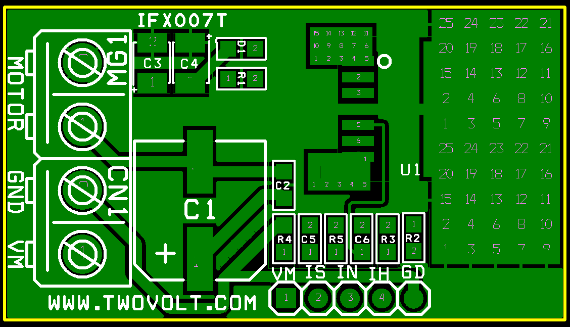
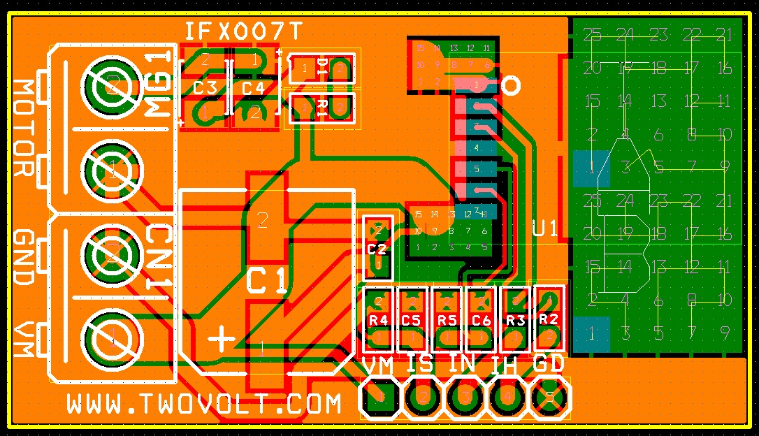
The High Current DC Motor driver project has been designed using IFX007T IC from infinion, The project can drive large size brushed DC motor , speed control is easy using PWM , the board also has few features like short circuit protection, over temperature and over current protection, its provide current feedback can be interface with arduino , raspberry pai. Motor connections and DC supply input possible using screw terminals, all inputs can be feed using 5 pin male header connector, onboard power LED, The IFX007T is an integrated high current half bridge for motor drive applications. It is part of the Industrial & Multi-Purpose Nova lithic™ family containing one p-channel high-side MOSFET and one n-channel low-side MOSFET with an integrated driver IC in one package. Due to the p channel high-side switch the need for a charge pump is eliminated thus minimizing EMI. Interfacing to a micro controller is made easy by the integrated driver IC which features logic level inputs, diagnosis with current sense, slew rate adjustment, dead time generation and protection against over temperature, under voltage, over current and short circuit. The IFX007T provides a cost optimized solution for protected high current PWM motor drives with very low board space consumption.Download PDF Schematic.
The IFX007T is part of the Industrial & Multi Purpose NovalithIC™ family containing three separate chips in one package: One p-channel high-side MOSFET and one n-channel low-side MOSFET together with a driver IC, forming an integrated high current half-bridge. All three chips are mounted on one common lead frame, using the chip-on chip and chip-by-chip technology. The power switches utilize vertical MOS technologies to ensure optimum on state resistance. Due to the p-channel high-side switch the need for a charge pump is eliminated thus minimizing EMI. Interfacing to a microcontroller is made easy by the integrated driver IC which features logic level inputs, diagnosis with current sense, slew rate adjustment, dead time generation and protection against over temperature, under voltage, overcurrent and short circuit. The IFX007T can be combined with other IFX007Ts to form a H-bridge or a3-phase drive configuration.
Features
- Operation up to 40 V
- Current limitation level of 55 A min.
- Path resistance of max. 12.8 mΩ @ 25°C (typ. 10.0 mΩ @ 25°C)
- High side: max. 6.5 mΩ @ 25°C (typ. 5.3 mΩ @ 25°C)
- Low side: max. 6.3 mΩ @ 25°C (typ. 4.7mΩ @ 25°C)
- Enhanced switching speed for reduced switching losses
- Capable for high PWM frequency combined with active freewheeling
- Switched mode current limitation for reduced power dissipation in over-current
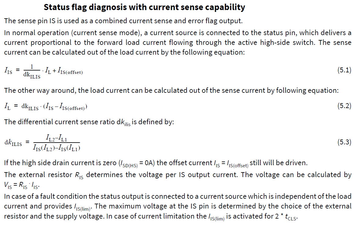
- Status flag diagnosis with current sense capability
- Over temperature shutdown with latch behavior
- Under-voltage shutdown
- Driver circuit with logic level inputs
- Adjustable slew rates for optimized EMI
- Green Product (RoHS compliant)
Short circuit protection
- The device provides embedded protection functions against
- output short circuit to ground
- output short circuit to supply voltage
- short circuit of load
- The short circuit protection is realized by the previously described current limitation in combination with the
- over temperature shutdown of the device.
Input circuit
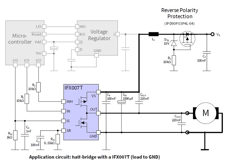
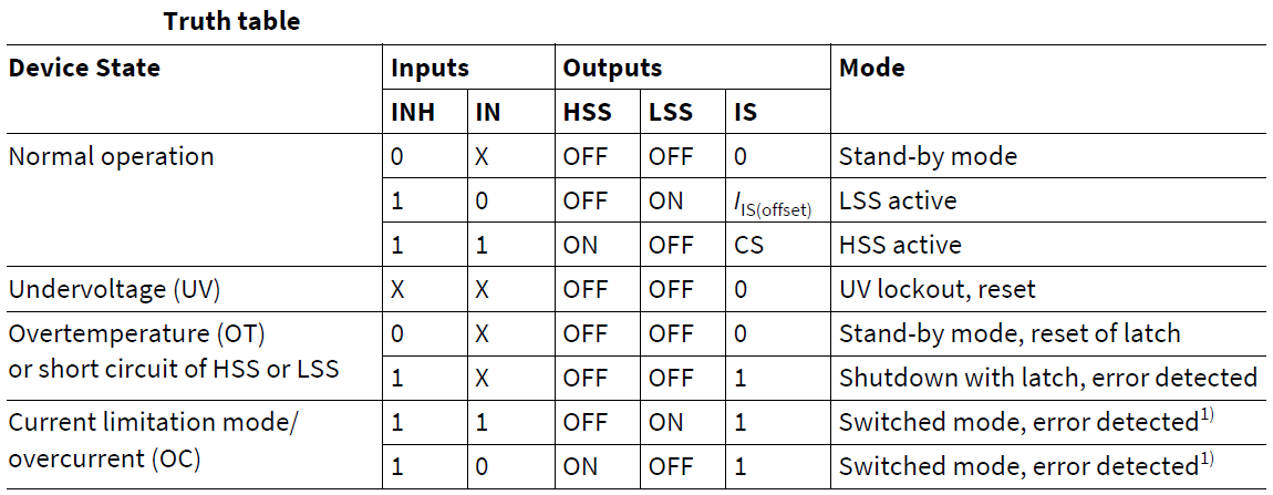
The control inputs IN and INH consist of TTL/CMOS compatible schmitt triggers with hysteresis which control the integrated gate drivers for the MOSFETs. Setting the INH pin to high enables the device. In this condition one of the two power switches is switched on depending on the status of the IN pin. To deactivate both switches, the INH pin has to be set to low. No external driver is needed. The IFX007T can be interfaced directly to a microcontroller
Dead time generation
In bridge applications it has to be assured that the high-side and low-side MOSFET are not conducting at the same time, connecting directly the battery voltage to GND. This is assured by a circuit in the driver IC, generating a so called dead time between switching off one MOSFET and switching on the other. The dead time generated in the driver IC is automatically adjusted to the selected slew rate.
Adjustable slew rate
In order to optimize electromagnetic emission, the switching speed of the MOSFETs is adjustable by an external resistor. The slew rate pin SR allows the user to optimize the balance between emission and power dissipation within his own application by connecting an external resistor RSR to GND
PWM control
For the selection of the max. PWM frequency the choosen rise/fall-time and the requirements on the duty cycle have to be taken into account. We recommend a PWM-period at least 10 times the rise-time.
Example:
Rise-time = fall-time = 4 μs.
=> T-PWM = 10 * 4 μs = 40 μs.
=> f-PWM = 25 kHz.
The min. and max. value of the duty cycle (PWM ON to OFF percentage) is determined by the real fall time plus the real rise time. In this example a duty cycle make sense from approximately 20% to 80%. If a wider duty cycle range is needed, the PWM frequency could be decreased and/or the rise/fall-time could be accelerated.