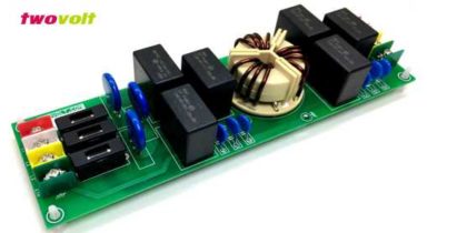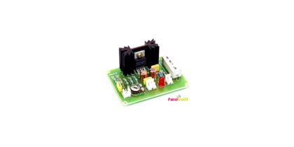
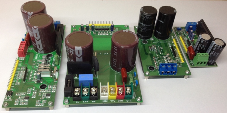
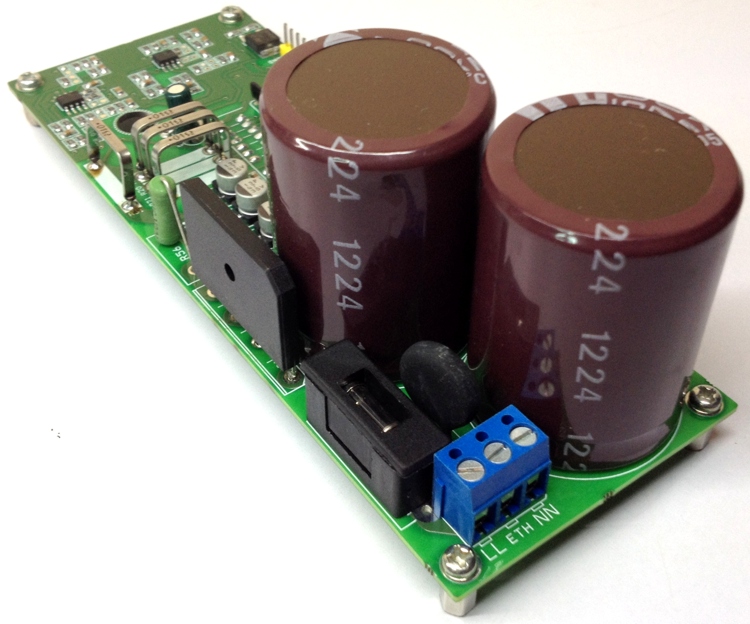
1.6KW Brush-Less Motor Power Driver Using IPM STK554U362
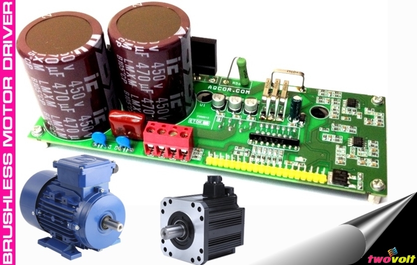
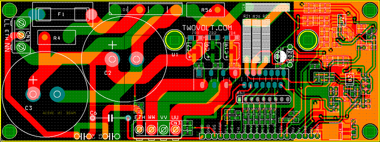
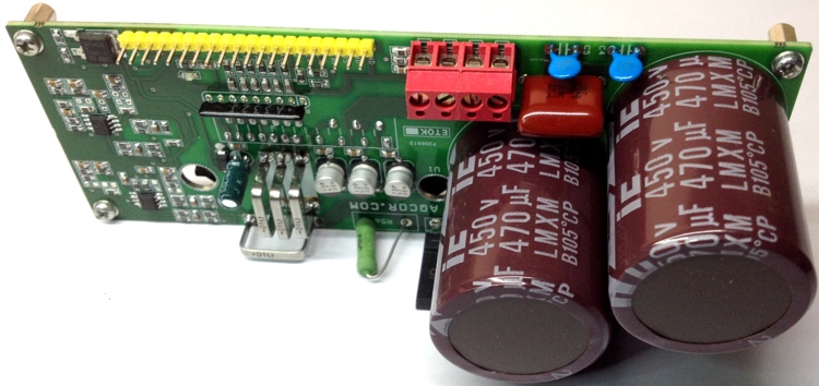
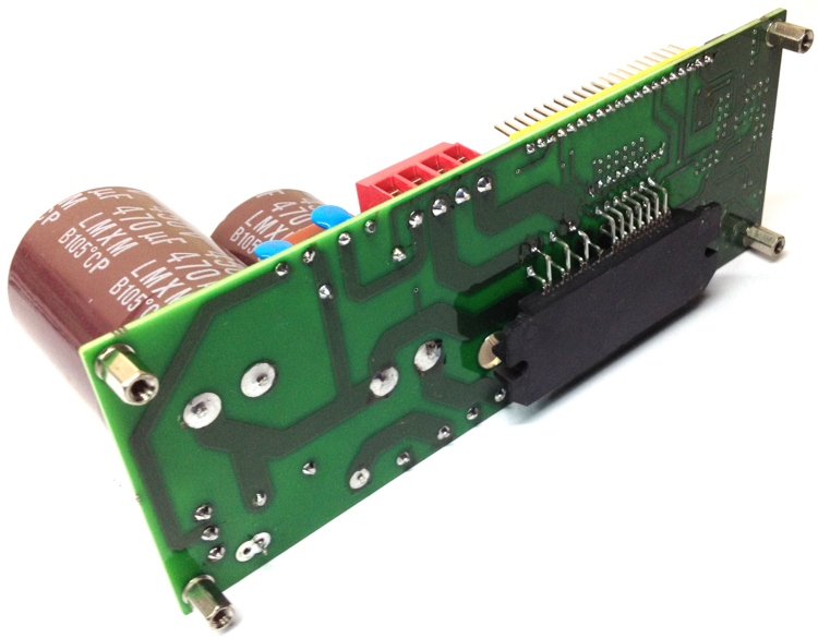
The compact motor drive power board is based on STK554U362A IPM module from ON semiconductor. It provides an affordable and easy-to-use solution for driving high power Brushless servo, AC Motors, and DC Brushless motors in a wide range of applications such as power white goods, air conditioning, compressors, power fans, high-end power tools and 3-phase inverters for motor drives in general.
The IPM itself consists of short-circuit rugged IGBTs and a wide range of features like (UVP) under voltage protection, (OCP) Over current protection with fault detection output flag , embedded temperature sensor NTC.Internal Boost diodes are provided for high side gate boost drive.
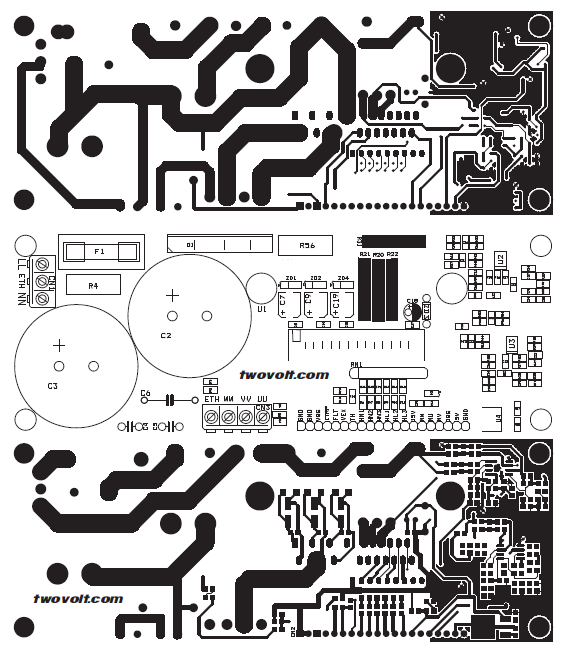
The main characteristics of this project are its small size, minimal BOM and high efficiency. It consists of an interface circuit, bootstrap capacitors, fault event signal and temperature monitoring. It is designed to work in single or three shunt configuration and with dual current sensing options: using three dedicated on-board op-amps
Thanks to these advanced characteristics, the system can provide the fast and accurate current feedback conditioning necessary for field oriented control (FOC). Refer Data sheet for more information
- Input voltage: 125 to 400 VAC
- Nominal power: up to 1600 W
- Nominal current: up to 10 A
- Input auxiliary voltage: up to 20 VDC
- On Board 5V Regulator for Op-Supply
- D2 Power LED (Gate Driver Supply)
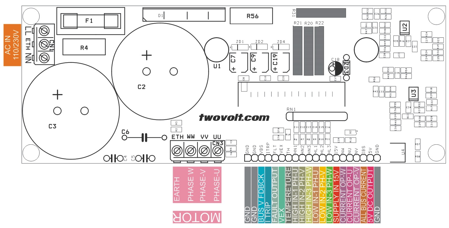
- 3 Pin Screw Terminal for AC Supply Input
- 4 Pin Screw Terminal Connector For Motor Connections
- On Board Fuse for Short Circuit Protection
- Single- or three- shunt resistors for current sensing
- IPM temperature monitoring and protection
- Highly integrated device containing all High Voltage (HV) control from HV-DC to 3-phase outputs in a single small SIP module.
- Output stage uses IGBT/FRD technology and implements Under Voltage Protection (UVP) and Over Current Protection (OCP) with a Fault Detection output flag. Internal Boost diodes are provided for high side gate boost drive.
- 3 Independent shunt resistors and 3 X Channel signal condition amplifiers help to easy FOC based driver
- Header connector provided for inputs and logic supply input
- Externally accessible embedded thermistor for substrate temperature measurement.
- Single control power supply due to internal bootstrap circuit for high side pre-driver circuit.
- Externally accessible embedded thermistor for substrate temperature measurement.
- All control inputs and status outputs are at low voltage levels directly compatible with micro-controllers.
Note : This board also supports following ICs
- STK554U362 10A Load DOWNLOAD DATA SHEET
- STK554U392 15A Load DOWNLOAD DATA SHEET
- STK554U3A2A-E 20A Load DOWNLOAD DATA SHEET
![]()

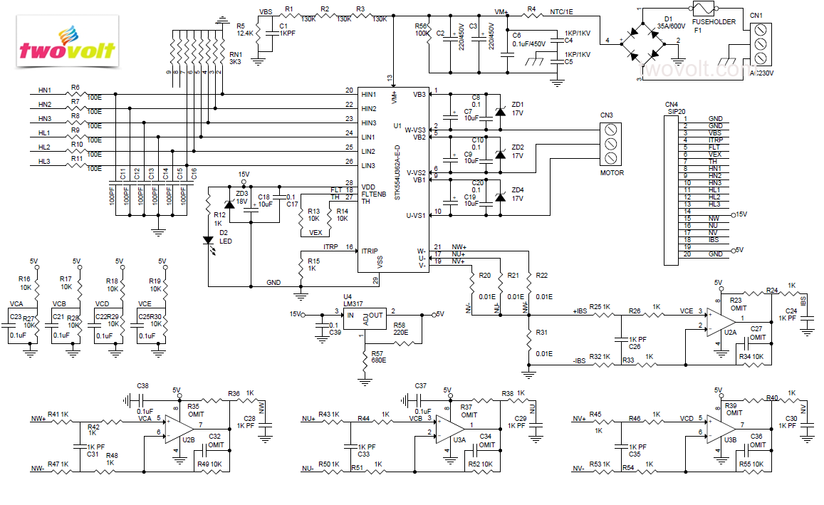
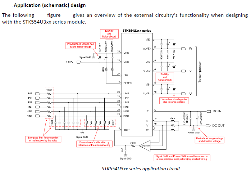
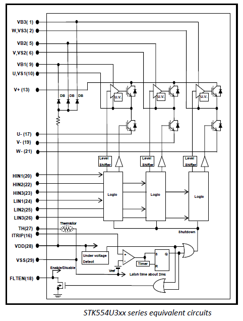
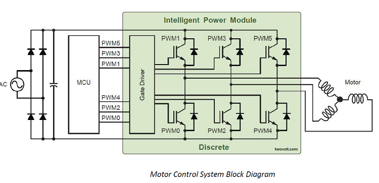
TheSTK554U362A is Intelligent Power Module (IPM) based upon ONs Insulated Metal Substrate Technology (IMST) for 3-phase motor drives which contain the main power circuitry and the supporting control circuitry. The key functions are outlined below:
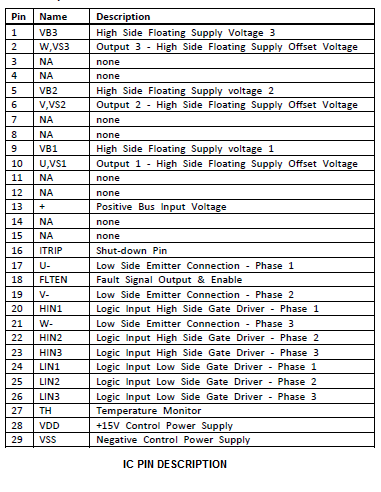
IC PIN FUNCTIONS
+, U-, V-, W-
These pins are connected with the main DC power supply. The applied voltage is up to the Vcc level. Overvoltage on these pins could be generated by voltage spikes during switching at the floating inductance of the wiring. To avoid this behavior the wire trac-es need to be as short as possible to reduce the floating inductance. In addition a snubber capacitor needs to be placed as close as possible to these pins to stabilize the voltage and absorb voltage surges.
U, V, W
These terminals are the output pins for connecting the 3-phase motor. They share the same GND potential with each of the high side control power supplies. Therefore they are also used to connect the GND of the bootstrap capacitors. These bootstrap capaci-tors should be placed as close to the module as possible.
VDD, VSS
These pins connect with the circuitry of the internal protection and pre-drivers for the low-side power elements and also with the control power supply of the logic circuitry. Voltage to input these terminals is monitored by the under voltage protection circuit. The VSS terminal is the reference voltage for the control inputs signals.
VB1, VB2, VB3
The VBx pins are internally connected to the positive supply of the high-side drivers. The supply needs to be floating and electrically isolated. The boot-strap circuit shown in Figure 20 forms this power supply individually for every phase. Due to integrated boot resistor and diode (RB & DB) only an external boot capacitor (CB) is required.
CB is charged when the following two conditions are met. ① Low-side signal is input ② Motor terminal voltage is low level
The capacitor is discharged while the high-side driver is activated.
Thus CB needs to be selected taking the maximum on time of the high side and the switching frequency into account.
The voltages on the high side drivers are individually monitored by the under voltage protection circuit. In case an UVP event is detected on a phase its operation is stopped.
Typically a CB value of less or equal 47uF (±20%) is used. In case the CB value needs to be higher an external resistor (of apx. 20Ω or less) should be used in series with the capacitor to avoid high currents which can cause malfunction of the IPM.
HIN1, LIN1, HIN2, LIN2, HIN3, LIN3
These pins are the control inputs for the power stages. The inputs on HIN1/HIN2/HIN3 control the high-side transistors of U/V/W, and the inputs on LIN1/LIN2/LIN3 control the low-side transistors of U/V/W respectively. The input are active high and the input thresholds VIH and VIL are 5V compatible to allow direct control with a microcontroller system
Simultaneous activation of both low and high side is prevented internally to avoid shoot through at the power stage. However, due to IGBT switching delays the control signals must include a dead-time.
For fail safe operation the control inputs are internally tied to VSS via a 33kΩ (typ) re-sistor. To avoid switching captured by external wiring to influence the module behavior an additional external low-ohmic pull-down resistor with a value of 2.2kΩ-3.3kΩ should be used.
The output might not respond when the width of the input pulse is less than 1μs (both ON and OFF).
FLTEN
The FLTEN pin is an active low input and open-drain output. It is used to indicate an in-ternal fault condition of the module and also can be used to disable the module opera-tion. The I/O structure is shown
The internal sink current IoSD during an active fault is nominal 2mA @ 0.1V. Depending on the interface supply voltage the external pull-up resistor (RP) needs to be selected to set the low voltage below the VIL trip level.
For the commonly used supplies VP:
VP = 15V -> RP >= 20kΩ VP = 5V -> RP>= 6.8kΩ
For a detailed description of the fault operation refer data sheet chapter 4
Note: The Fault signal does not latch permanently. After the protection event ended and the fault clear time(2ms) passed, the module operation is automatically re-started. Therefore the input needs to be driven low externally activated as soon as a fault is detected.
TH
An internal thermistor to sense the substrate temperature is connected between TH and VSS. By connecting an external pull-up resistor to arbitrary voltage, the module temperature can be monitored. Please refer to heading 3.2 for details of the thermis-tor.
Note: This is the only means to monitor the substrate temperature indirectly.
Operation procedure
Step1: Please connect IPM, each power supply, logic parts, and the motor to the evaluation board,
and confirm that each power supply is OFF at this time.
Step2: Please impress the power supply of DC15V.
Step3: Please perform a voltage setup according to specifications, and impress the power supply
between the “+” and the “-” terminal.
Step4: By inputting signal to the logic part, IPM control is started.
(Therefore, please set electric charge to the boot-strap capacitor of upper side to turn on
lower side IGBT before running.)
* When turning off the power supply part and the logic part, please carry out in the reverse order
to above steps.